
Page 72 - Roadmap
P. 72
8.4. PHYSICAL SCIENCES AND ENGINEERING
Nano-characterization laboratory for the development of new advanced materials
Instruments Centre, Faculty of Science, Eötvös Loránd University
Project code: Project description:
VEKOP-2.3.3.-15-2016-0003 Changes in the microstructure of structural materials during use have a decisive im-
pact on their usability. So, it is essential to have a thorough understanding of mi-
Project leader institution: crostructures for the development of new advanced materials and for the
Faculty of Science, Eötvös Loránd determination of their life cycle. The ELTE TTK microstructure research laboratory
University features three devices that can determine microstructure at three different scales
(atomic, nano and micro).
Project leader:
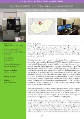
István Groma The largest device is unique in Hungary: the FEI Quanta 3D scanning electron mi-
croscope has a high-resolution dual beam (SEM/FIB) apparatus. Dual beam means
Project leader’s contacts: that it has both electron and ion sources. Both beams are suitable for capturing mi-
groma@metal.elte.hu croscopic images but the ion beam makes it possible to manipulate the surface of the
sample material at nanoscale. The equipment has several detectors: Secondary elec-
Amount of funding: trons have the smallest energy resulting ~1 nm resolution. Backscattered electrons
HUF 155,595,855 have somewhat higher energy, so they provide information from deeper levels at a
resolution of ~2 to 4 nm. The energy of X-ray photons reveal information on their
RI type: Single-site source atom. Therefore, by measuring the energy of the collected X-ray photons, we
can analyze the chemical composition of the sample at a certain point or along its
Website: surface. The equipment can also operate in transmission mode (STEM) and it is ca-
http://sem.elte.hu pable to measure electron backscatter diffraction (EBSD) image allowing to deter-
mine the local crystalline orientation.
The atomic level structure of surfaces can be imaged by the newly acquired Integrated
Scanning Tools for HORIBA Advanced Nano-Technology SmartSPM SPMTM-
1000, which works in non-contact AFM, contact AFM, Kelvin probe force mi-
croscopy, Piezo response force microscopy, STM, magnetic force microscopy and
shear force microscopy modes and it is suitable for nanolithography.
The RIGAKU SmartLab X-ray diffractometer purchased in the same project is
equipped with a highly advanced detector and control unit. It enables traditional
powder diffraction measurements for determining the phases present in the sample,
as well as the determination of texture by inserting a moving/rotating table. It also
makes possible to perform X-ray line profile measurements for the direct determi-
nation of several microstructure parameters (particle size, dislocation density etc.).
72